Amiga 1200 Keyboard, part 3
Drawing the schematic.
In the last part the circuit was derived by tracing the membrane in the original A1200 keyboard. This time that circuit is going to be turned into a schematic drawing, with the output being a netlist - simply, a list of pins connected to parts (keyswitches, LED, connector) that are connected together.
Because it makes for nice organisation they keys in the schematic go in roughly the same place they would be on a real keyboard. Compared to making a PCB schematic is not hard at all - wires can cross and go pretty much anywhere as long as you can keep track of them. Unless you see a big green dot you don't have a connection. Obviously you don't want to make something you can't read so keeping it neat is a good idea.
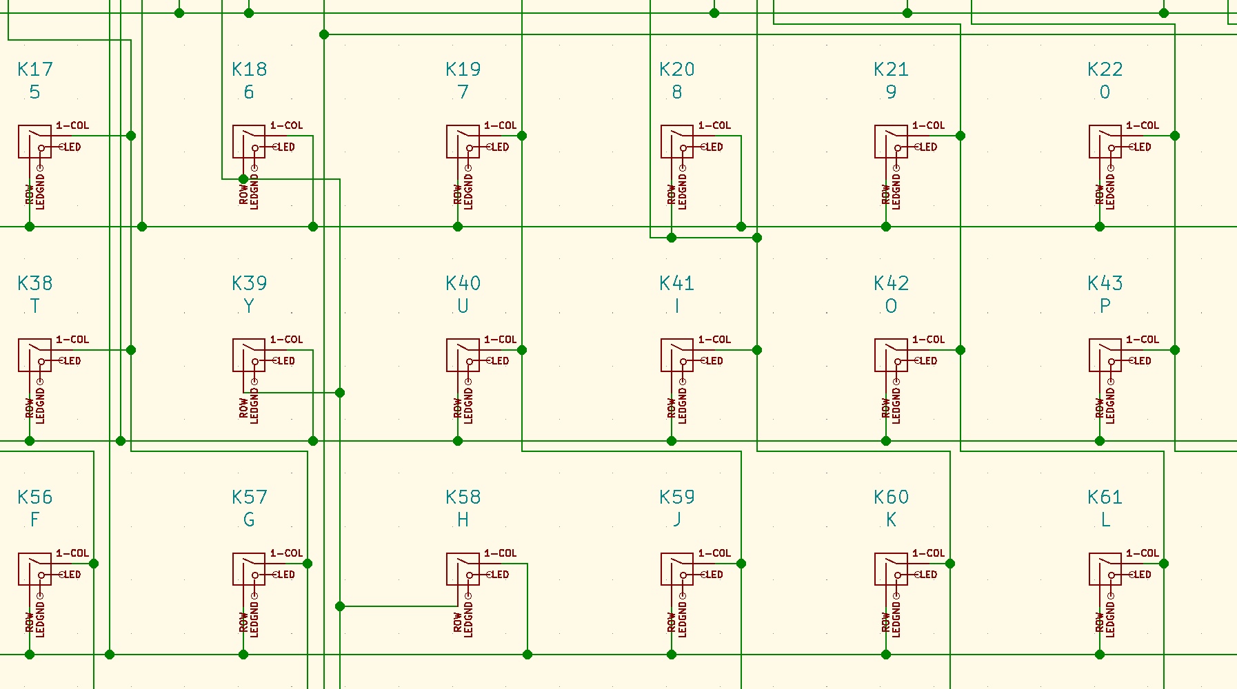
Looking at the circuit you can see that it is a matrix. The keys, with two terminals each, could be directly connected to the controller, for around 200 connections from keyboard to controller. Or like a joystick they could all use one common connection and then there would only be 100 wires or so, one from each switch plus one common. But better still is to use a matrix where a key is defined by two connections, and when those connections are bridged the controller derives a unique key. The minimum you would need is rows + columns connections - so in a really simple keyboard like this standalone numpad:
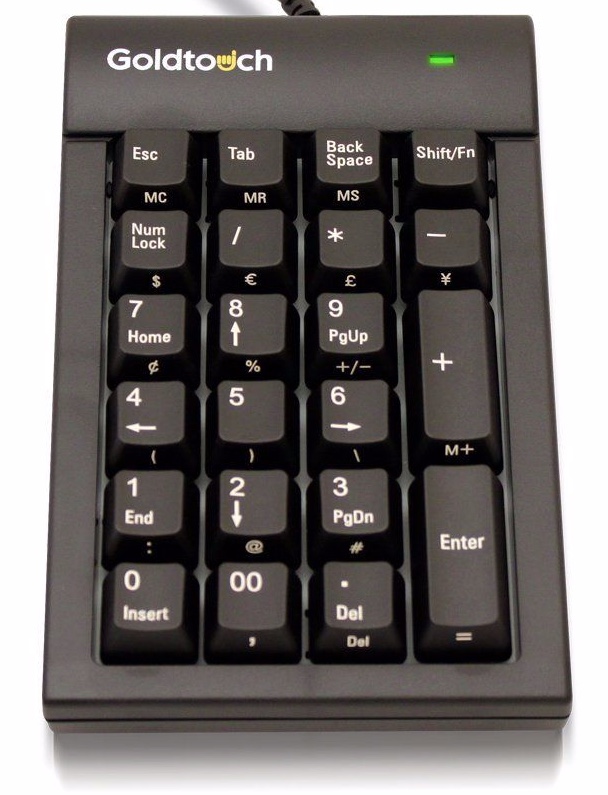
The minimum would be only 10 connections from matrix to controller because there are 4 column and 6 rows. All this minimisation is good because connections cost time and money. The Amiga however has a special set of keys with their own connections not shared with the regular matrix. These are keys like CTRL, L-AMIGA etc - the ones that can't be blocked by another key. Ignoring the connections to the LED that lights when CAPSLOCK is pressed it uses 29 connections to the controller chip, via the ribbon cable that emerges from the top of the membrane.
I could write a whole article about the keyboard matrix and try to make it good, but it's been done really well already - please take a look at komar's tech blog.
Because I just want to make a replacement keyboard I am not using diodes or changing the layout in any way from the original. The circuit is exactly the same right down to the flipped row/column connections on some of the keys like F6. I do not think that making all this completely regular could have had an effect, as these are just passive switches, but I'm not changing it. The keyboard should be better with mechanical switches, but it should not be electrically different - bugs and all.
When the schematic is done the output is a netlist. This is just a text file that defines what's in the circuit and how the things are connected. The first part describes the components. Here are two entries (and part of a third) describing the switches:
  (components
    (comp (ref K2)
      (value F1)
      (footprint MX_Alps_Hybrid:MXOnly-1.25U-NoLED)
      (libsource (lib MX_Alps_Hybrids) (part MX-1.25U) (description ""))
      (sheetpath (names /) (tstamps /))
      (tstamp 5C7001B7))
    (comp (ref K3)
      (value F2)
      (footprint MX_Alps_Hybrid:MXOnly-1.25U-NoLED)
      (libsource (lib MX_Alps_Hybrids) (part MX-1.25U) (description ""))
      (sheetpath (names /) (tstamps /))
      (tstamp 5C70020E))
    (comp (ref K4)
      (value F3)
      (footprint MX_Alps_Hybrid:MXOnly-1.25U-NoLED)
      (libsource (lib MX_Alps_Hybrids) (part MX-1.25U) (description ""))
I'm using the excellent library by github user ai03-2725 - highly recommended. I don't love the schematic symbols, because all of the keys have a diode which when unconnected causes KiCAD to complain when transferring to PC. But the PCB footprints are excellent!
Late in the netlist comes the description of the nets themselves - here's one of them:
    (net (code 198) (name /18)
      (node (ref K36) (pin 1))
      (node (ref K55) (pin 1))
      (node (ref K3) (pin 1))
      (node (ref J1) (pin 18))
      (node (ref K74) (pin 1))
      (node (ref K15) (pin 1))
      (node (ref K68) (pin 1)))
This means that there is a net named "18", joining the pins of the components listed. I named is "18" because it matches pin 18 of the connector. And it's as simple as that. If you look at the netlist file you can manually check that all of the nets are connected the way you wanted them. This is a good idea because though it is not an exciting job it's a lot better than soldering bits of wire on your new PCB correcting in hardware the errors you should have fixed on paper.
Next time - making the PCB.