Amiga 1200 Keyboard, part 5
Making the PCB.
One weekend morning I got up thinking it was time to get this done! Could I use an autorouter? It would be quick, and the first rev isn't going to be perfect. Plenty of time for making a pretty hand route later as there would be things to fix, surely?
But no. KiCAD and autorouters don't really mix any more. Once upon a time the ability to use an autorouter was in KiCAD although the routing code itself wasn't; the idea being that you install a .JAR file containing the autorouter code, export a Specctra Design (.DSN) file from KiCAD, click the menu item and the routed PCB is done. There are a few web sites about it from a few years ago. In the end it didn't work for me and I wasted a couple of hours I could have used routing the board. The stories of success are just a little too old and too many small details have changed.
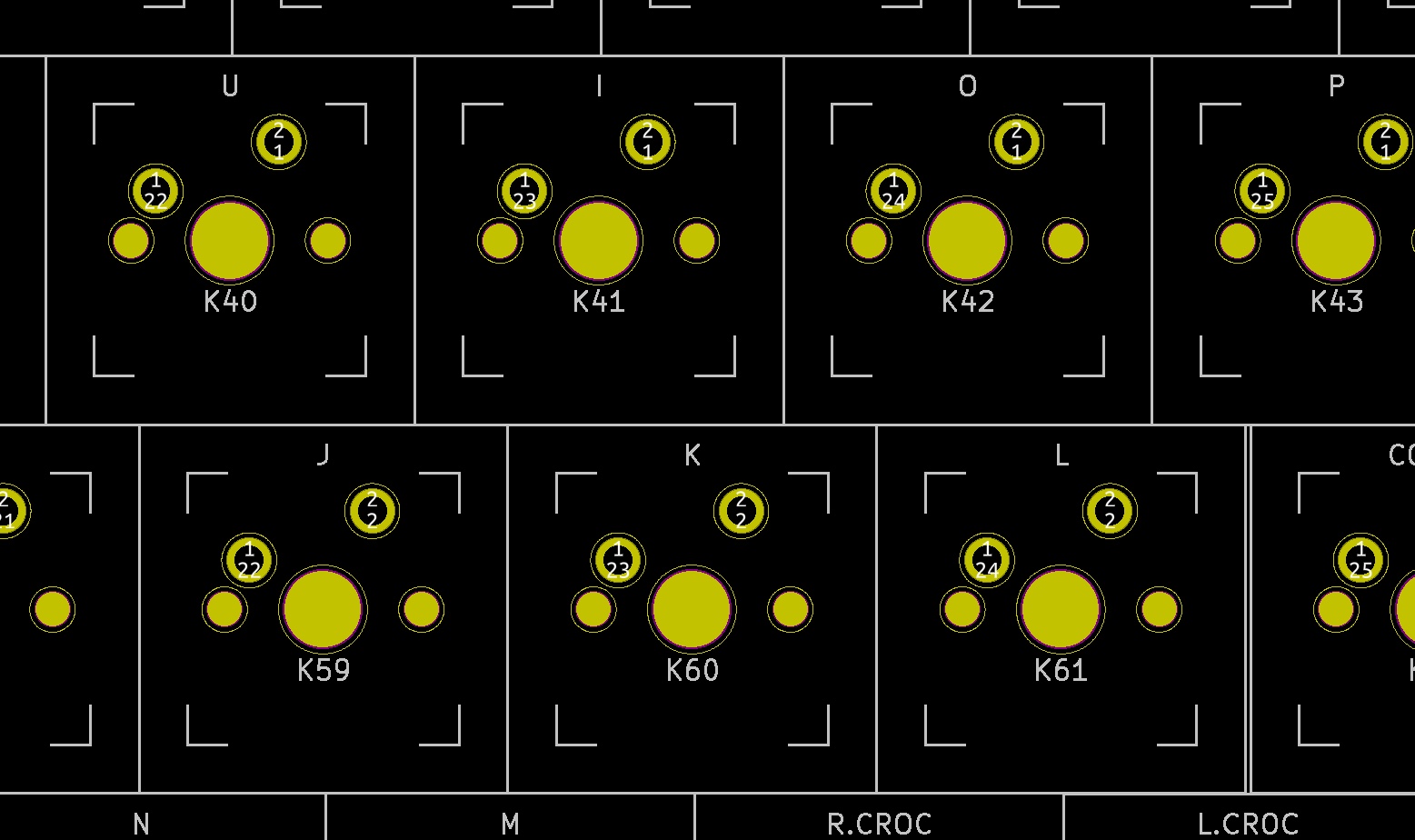
Using the fantastic MX footprints included in the KiCAD library from ai03-2725 made placing the switches in the right place easy. One box is placed next to another - 'E' key next to 'W' key and so on. Soon all the keys are in place, according to my measured offsets (see last article).
Before geting started you set up the basic board parameters and design rules. I need to pass traces through between the pins of the FFC connector, so my smallest trace needs to be 0.35mm. The PCB maker has a question when placing an order and it looks like things begin to get more expensive when a hole is less than 0.60mm - so I'll use 0.60.

Routing a board in KiCAD is a lot like every other PCB package I have used. It starts with a rats nest display, which really doesn't tell you anything except that nothing is connected, so you hide it. Select the layer on which you want to place a track. Click on one point to connect and the line will drag out, interactively routing itself around things it can't be connected to. If you try and put the trace between two pins that are too close together it just won't go there, instead it will route itself all over the board in an effort to get there. The end result is that you end up with a circuit with no design rule violations. I have used a system that could highlight the places tracks got too close, but you could still make the mistake and violate your own rules. I have also used a system with no checking and it's only when you get the PCB back you find the wrong things are connected. Overall, the KiCAD interactive router is good.
For rev 1 of the board I tried to use no vias with two layers - not because it matters but because when making a PCB years ago I was told vias make the board more expensive. In the end I think there are threein total, so not bad. But this is a little like writing code in 2019 and using lookup tables and integer approximations for trigonometry, because sinf() is so slow! In fact sinf() is fast now, faster than your lookup table, and in same way the number of vias no longer matters. Don't waste your time.
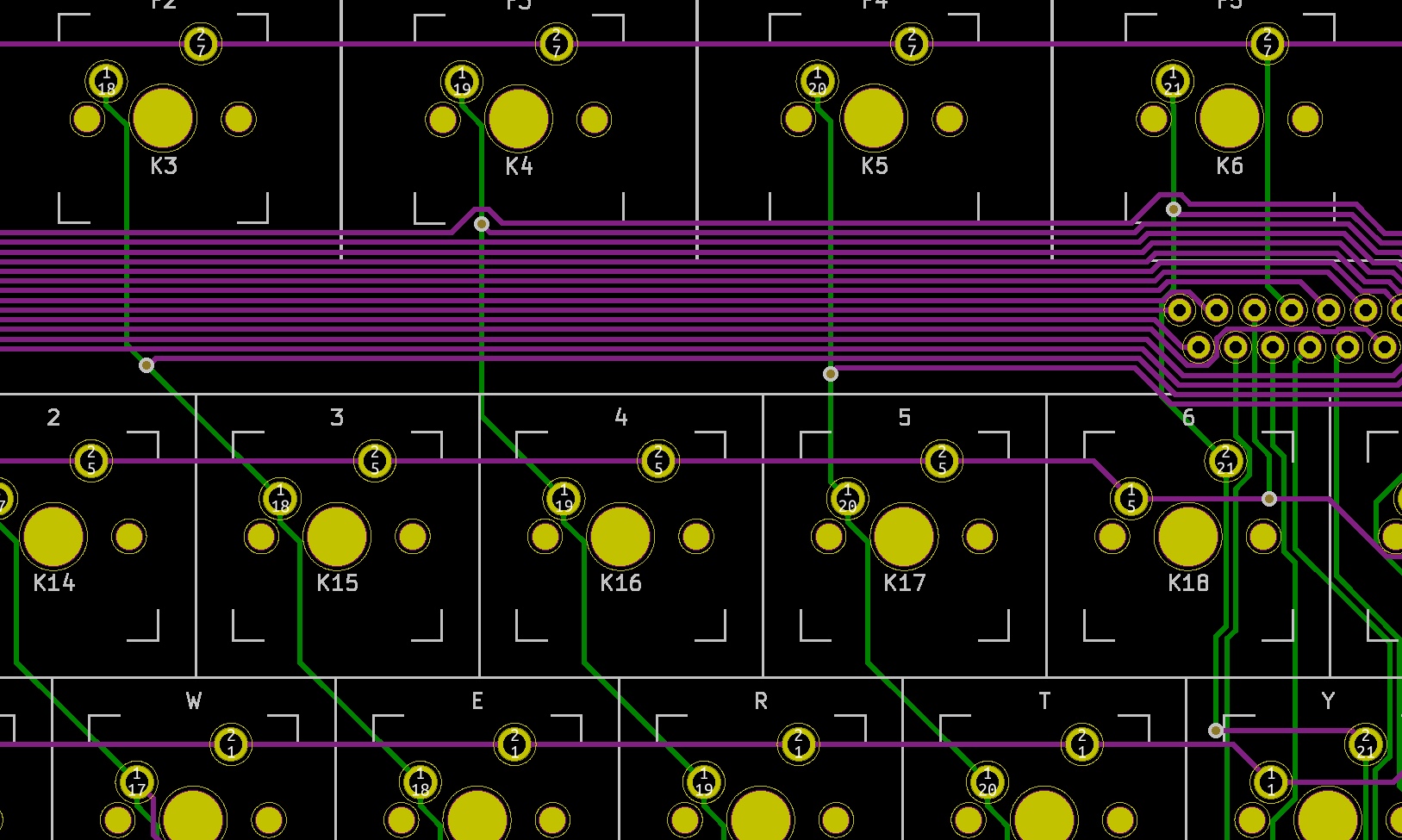
What you should do is use vias wherever you need them. Above I said "two layers", meaning there are copper tracks on the front and the back of the PCB. Between those layers the holes that the component pins go through are plated through, so both sides are electrically connected. So a trace can come up to a pin on the front of the board, and another trace can go away from that pin on the rear of the board and they will be electrically connected. If you want a trace to switch sides without going to a pin first, you use a via which is really just a through hole that no component will go in.
When routing it is a good idea to keep your options open. No sooner do you make a trace hug close to the existing routing to keep plenty of space on one side then you find you need space on the side you took it all away from. Also you need to be able to move long distances without thinking too hard and as the board gets more crowded it can be impossible. If you try to make all your connections more or less direct then soon you have created a maze that can't be solved. My solution to this is to make one layer (top) run mostly east-west, and the other layer (bottom) run north-south. If the trace has to change direction, use a via rather than allowing a trace on one layer to fence in other connections. This problem gets dramatically worse once many connections have been made.
Once done - and you're sure it's right - it's time to submit the job to the manufacturer. You don't "export" this, you "plot" it. In the olden days that's how they used to do it (I have read) and all the PCB software still calls it "plot", and you make "gerbers" - not baby food, not legendary blades, but the RS-274X file format. These describe the layers that need to be made with various processes to make your board. There is the copper (both sides), the mask (the paint-like stuff that covers all the copper that should not be exposed), the board outline (where the board will be cut out) and the silk screen. This last one is not essential but very useful for including information on the board like where to place components.
The service I am using is called OurPCB. It looks easy - there is a list of things to choose, like the weight of the substrate material, copper thickness, the board size, how many you want made, how fast, and many other things. Then it tells you how much this will cost. It's real money alright but nothing like as expensive as this used to be.
About 20 minutes after submitting the order I got an email back saying that one of my files (solder mask) was missing. I submitted that and all was well. Great service! OurPCB is highly recommended.
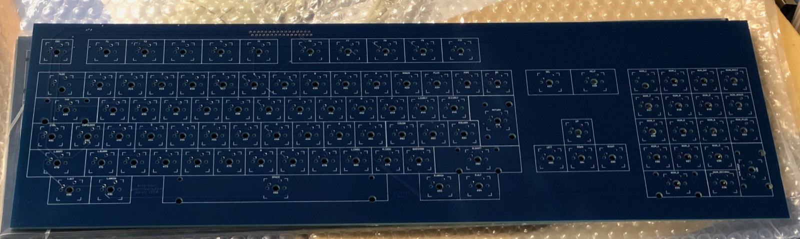
About 8 days later, right on time, I got a delivery at work - PCBs. The next article will be all about adding components and making it fit into the computer.